Silicon Sheet Resistance

2 9 Mobility Resistivity Sheet Resistance
General Properties Of Silicon Pveducation
Https Www Jkps Or Kr Journal Download Pdf Php Spage 630 Volume 45 Number 9 6

Module 4

Sheet Resistance An Overview Sciencedirect Topics
2 Semiconductor Doping Technology

And y the distance between two grid fingers as shown below.
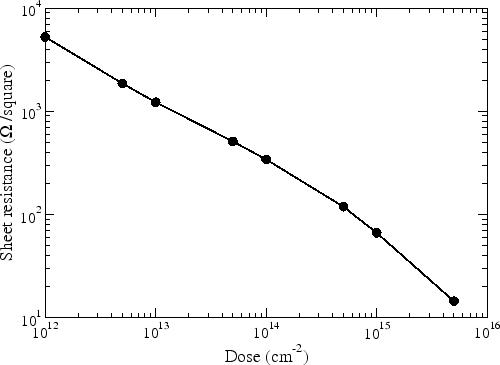
Silicon sheet resistance. The mobility of electrons and holes in bulk silicon is shown in the figure below. This calculator determines the sheet resistance of an arbitrarily doped semiconductor at equilibrium. Semiconductor devices depend on the distribution of carriers electrons or holes within their structures to provide the desired performance the carrier concentration which can vary by up to ten orders of magnitude can be inferred. The calculator simulates a four point probe measurement of a surface diffusion such as an emitter a back surface field or a front surface field of a photovoltaic pv solar cell.
Veli matti airaksinen in handbook of silicon based mems materials and technologies second edition 2015. Spreading resistance profiling srp also known as spreading resistance analysis sra is a technique used to analyze resistivity versus depth in semiconductors. An inductive circuit generates a high frequency magnetic field which causes circulating eddy currents in the wafer. For example for a typical silicon solar cell where.
Hello sheet resistance also known as surface resistance or surface resistivity is a common electrical property used to characterize thin films of conducting and semiconducting materials. Filmetrics sheet resistance measurement tools marry the technology developed and perfected by kla for over 30 years with the bench top instrument technology developed over the last 20 years by the filmetrics team. Kla technologies include both contact and non contact methods. Sheet resistance measurements of bulk silicon wafers are commonly done with an eddy current gauge.
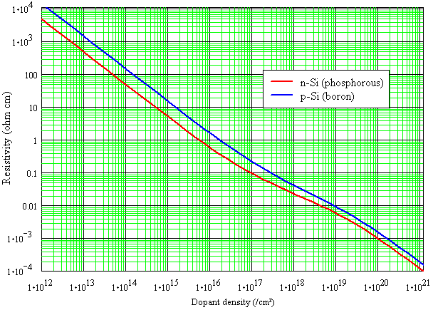
Resistiv xls mobility gif fig 2 9 1 electron and hole mobility versus doping density for silicon. The sheet resistivity of an emitter layer is typically measured with a four point probe. The differential resistance is given by. Sheet resistance often called sheet resistivity is a measure of resistance of thin films that are nominally uniform in thickness.
The resistance of a square conductive sheet is the same no matter what size it is so long as it remains a square. The term ohms per square is used when measuring sheet resistance i e the resistance value of a thin layer of a semi conductive material. This is an active figure which can be used to find the bulk mobility for specific doping concentrations as well as the related resisitivity and sheet resistance. For non uniformly doped n type layers ie if ρ is non uniform.
It is commonly used to characterize materials made by semiconductor doping metal deposition resistive paste printing and glass coating examples of these processes are. The user can either generate a dopant profile or upload a profile from a sims ecv or spreading resistance.
Sheet Resistivity
Emitter Layer Formation By Spin On Doping On Mono Crystalline

Sheet Resistance Calculator

Spreading Resistance Profiling Wikipedia

Pdf Unexpectedly High Etching Rate Of Highly Doped N Type

Pdf Chemical Treatment Of Crystalline Silicon Solar Cells As A

Silicon Steel An Overview Sciencedirect Topics

Monocrystalline Silicon Solar Cell Sample Structure Download

Anodic Oxidations Excellent Process Durability And Surface

Pdf Infrared Radiative Properties Of Heavily Doped Silicon At

Dielectric Surface Passivation For Silicon Solar Cells A Review
Monolithic Perovskite Silicon Homojunction Tandem Solar Cell With

Pdf Materials For Microbolometers Vanadium Oxide Or Silicon
Bolometers An Overview Sciencedirect Topics
